
the field of business
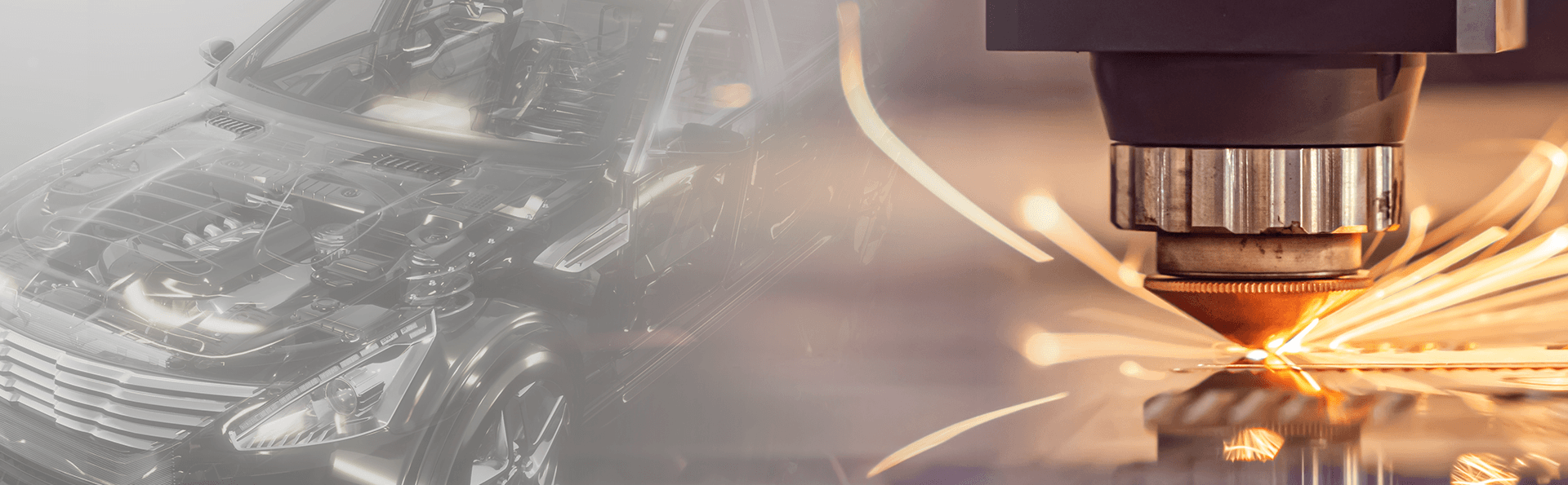
Wi-A laser division is conducting various application fields such as semiconductors, displays, secondary batteries, and military laser oscillators
Laser department has the expertise and development process for semiconductors, displays, and secondary cell industry to providing various laser application fields.
Wi-A laser division is conducting various application fields such as semiconductors, displays, secondary batteries, and military laser oscillators
Application to various fields such as display and semiconductor industry using laser
.png)
.png)
.png)
.png)
.png)
.png)
.png)
.png)
.png)
.png)
.png)
.png)
.png)
.png)
.png)
.png)
.png)
.png)
.png)
.png)
.png)
.png)
.png)
.png)
.png)
.png)
.png)
.png)
.png)
.png)
.png)
-e.png)
.png)
.png)
.png)
.png)
.png)
.png)
.png)
.png)
.png)
.png)
.png)
.png)
.png)
.png)
.png)